Researchers have developed microscopic temperature sensors from novel 2D materials that are small enough to embed directly into processor chips. These sensors can detect temperature changes in just 100 nanoseconds and are over 100 times smaller than conventional designs, allowing for precise monitoring of localized hotspots.
The technology uses bimetallic thiophosphates, exploiting the free movement of ions under electrical current—a property typically avoided in transistors—for thermal sensing. This approach requires no extra circuitry and uses significantly less power than existing sensors.
While currently a proof of concept tested in a lab, the sensors address key limitations of external thermal monitoring. Their integration could enable more efficient, chip-level thermal management instead of conservative, core-wide throttling.
Main topics: New 2D material sensors, on-die thermal monitoring, faster and smaller temperature detection, proof-of-concept technology, potential applications in processor design.
Researchers build atom-thin 2D thermometers that can be embedded directly in processors — can detect temperature changes in 100 nanoseconds, millions of times faster than the blink of an eye
The 2D material sensors detect temperature changes in 100 nanoseconds and are over 100 times smaller than conventional designs.
Get Tom's Hardware's best news and in-depth reviews, straight to your inbox.
You are now subscribed
Your newsletter sign-up was successful
Penn State researchers have developed what they’re calling microscopic temperature sensors that are small enough to embed directly into processor chips, according to a paper published March 6 in Nature Sensors. The sensors, built from a novel class of two-dimensional materials, can detect temperature changes in 100 nanoseconds — millions of times faster than the blink of an eye, Penn State’s press release reads — and pack down to just one square micrometer, a size so small that thousands can be placed on a single chip.
Processors currently rely on temperature sensors placed outside the chip die itself, which limits the speed and precision of thermal monitoring. That gap’s important because individual transistors can spike in temperature faster than external sensors can register, forcing chips to apply conservative thermal throttling across entire cores rather than responding to localized hotspots. Penn State's design addresses that by integrating sensing directly into the silicon, using the same electrical currents already running through the chip.
The sensors are built from bimetallic thiophosphates, a two-dimensional material not previously used in thermal sensing. The material's key property is that its ions continue moving freely even when exposed to an electrical current. That’s a behavior that chip engineers normally try to eliminate in transistors, but the Penn State team exploited it instead, coupling ion transport for temperature detection with electron transport for reading that thermal data. The result is a sensor that the researchers claim requires no extra circuitry or signal converters and draws up to 80 times less power than conventional silicon-based thermal sensors.
"What is generally unwanted by industry in transistors is actually great for thermal sensing, so we really tried to exploit that in our design," said Saptarshi Das, professor of engineering science and mechanics at Penn State and corresponding author on the paper. “Rather than try to remove these ions from this system, we use them to our advantage," he goes on to explain, adding that coupling the ions for temperature sensing and electrons for reading that thermal data allowed the team to build an extremely accurate but compact device.
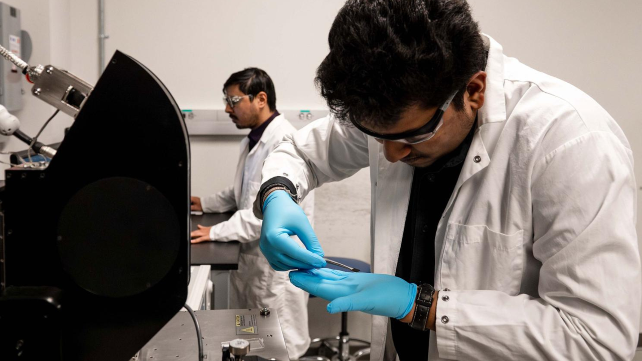
Das was clear, however, that the work is a proof of concept. While the sensors have been manufactured and tested in the lab using Penn State's Materials Research Institute Nanofabrication Laboratory, the path to commercial chip integration would require chipmakers to validate the process at scale. Still, the demonstrated specs — a 100-nanosecond response time, one square micrometer footprint, and no need for additional circuitry — address some of the constraints that have kept on-die thermal monitoring out of production silicon.
Follow Tom's Hardware on Google News, or add us as a preferred source, to get our latest news, analysis, & reviews in your feeds.
Get Tom's Hardware's best news and in-depth reviews, straight to your inbox.
Luke James is a freelance writer and journalist. Although his background is in legal, he has a personal interest in all things tech, especially hardware and microelectronics, and anything regulatory.
-
edzieba Reply"What is generally unwanted by industry in transistors is actually great for thermal sensing, so we really tried to exploit that in our design," said Saptarshi Das, professor of engineering science and mechanics at Penn State and corresponding author on the paper. “Rather than try to remove these ions from this system, we use them to our advantage," he goes on to explain, adding that coupling the ions for temperature sensing and electrons for reading that thermal data allowed the team to build an extremely accurate but compact device.
The big barrier to production implementation would be to be able to perform the required ion implantation for these sensors, whilst not 'poisoning' all of the surrounding transistors. If the sensors require a huge keep-out-zone around them, then the area they eat up starts to become a significant cost (both in terms of die area, and in actual cost with how high wafer prices are with newer processes).